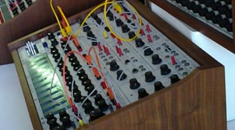
CBS Performance System 3 photo by Jen Castro. 410 module is the entire top half (5 module spaces).
Rick's photo of a 410 panel in the process of being cleaned:
http://www.flickr.com/photos/45430902@N07/6975855600/
Here is dgerrond's picture of the System 3:
http://www.flickr.com/photos/55624592@N04/9778396784/
NOTE: THIS IS NOT YET FULLY FUNCTIONAL. Will update as people share insight.
What is not finished and hopefully the community will chime in with answers so we can all enjoy this build?
-Pair of 2N4916 in the Ring Modulator; match them for gain or voltage or both?
-Pair of selected 2N4341 FETs in Ring Modulator, specified to be selected for two characteristics each: A Voff of between 3.0 and 6.0 as well as Rds matched at Vss = -1.35V. I cannot find such measuring procedures on the net. Need an easy test jig and procedure for these characteristics.
-The Envelope Detector is acting a bit strange; didn't find any trace mistakes...
-What is the value of R5 in the FFB? Illegible in the schematic. I installed a 100K pot across these pads and found that it sweeps the Fc, so this might be something to bring out to the front panel.
-The Filter is based upon lamps (not LEDs) and photoresistors, no idea what types/models. A pair of Vactrols "kinda" work. Also, I found I'd missed a 10R resistor in the ground path in the prototype; this release version includes a change to the artwork to attempt to include it but I'm unsure if I've succeeded in providing for whatever purpose it serves. Needs to be confirmed by someone who knows such things.
NOTE that there will be a second PCB (Reverb and Audio Power Amps) for this build and that it requires a spring reverb. No consideration has been taken regarding mounting a spring reverb unit behind a Buchla-style front panel, so it may not be possible to use this in 200e boats.
A panel is in discussion but will not be cheap as it is 5U Buchla format.
The Buchla 410 is a 5-space multi-function module which as far as I know only appeared in the CBS Performance System 3 (along with a 258A, 242 pulser, and a 216 touch keyboard). It is more "200" than "100" in that there are 741 opamps in most of the circuits as opposed to the 100 being for the most part, discrete.
I do not believe the CBS Performance System 3 even appears in the Buchla.com Historical section!
There is a lot less power in these 5 spaces than in an equivalent 200 series system but I'm drawn to the unusual choice of functions in the overall 3 instrument. Two oscillators, touch keyboard, programmable pulse source with VC clock, two preamps, envelope detector, reverb, two 20 watt audio power amps, two 3-channel mixers, two gates, an LDR lowpass VC filter, a four-channel fixed filter bank, ring modulator, noise, three envelopes...what music is this intended to produce?
CBS Performance System 3, via Don Hassler and Jason Butcher:
http://www.donhassler.com/jbutcher/blog/Ms3chaos.jpg
The upper section, a 5-space panel, is the model 410.
From left to right:
-Three AR envelopes with switching between one-shot and sustained
-Two VC Gates (VCAs) and Envelope Detector
-VC Filter, Reverb, Noise, Ring Modulator, Fixed Filter Bank (Input and four dual-jack outputs)
-Audio Power Amps and two Preamps
-Dual Three-Channel Mixers (no "All" mix output)
POWER:
The envelopes and envelope detector utilize +24 volts and produce a +15V output. The gates (VCAs) etc. are of course optimized to respond in this range. Mark Verbos discusses the changes to the Buchla voltage standards in his blog, buchlatech, so search it out. (The later 200 and now the 200e are +10V standard.)
This also means that later 200 and 200e modules will not produce enough CV to fully open the Filter or Gates on this board. Modifications can however be made to allow such...
The unit may work just fine with only a +24V source in addition to the +/-15V requirement. Part 2 will deal with the Reverb and Audio power amps which require +/-24V, and will live on a separate PCB. (Two +24V supplies may evidently be tied together to produce a bipolar output...)
Plug-In AC Adapters 24 VDC $8.36
Wiring a pair of +24 supplies for bipolar output (haven't tried this but should work) :
http://i.stack.imgur.com/iFt3B.png
SIGNAL LEVEL:
Seeing there is a 258A dual oscillator, I'll imagine it's slightly higher than the 100 series signal level and is perhaps into the range of the 200s, which is 1.2VRMS. Way below Eurack and Synthesizers.com/Modcan/Wiard etc. audio signal levels.
SCHEMATICS:
http://www.synthfool.com/docs/Buchla/410/
I recommend downloading and saving all of them.
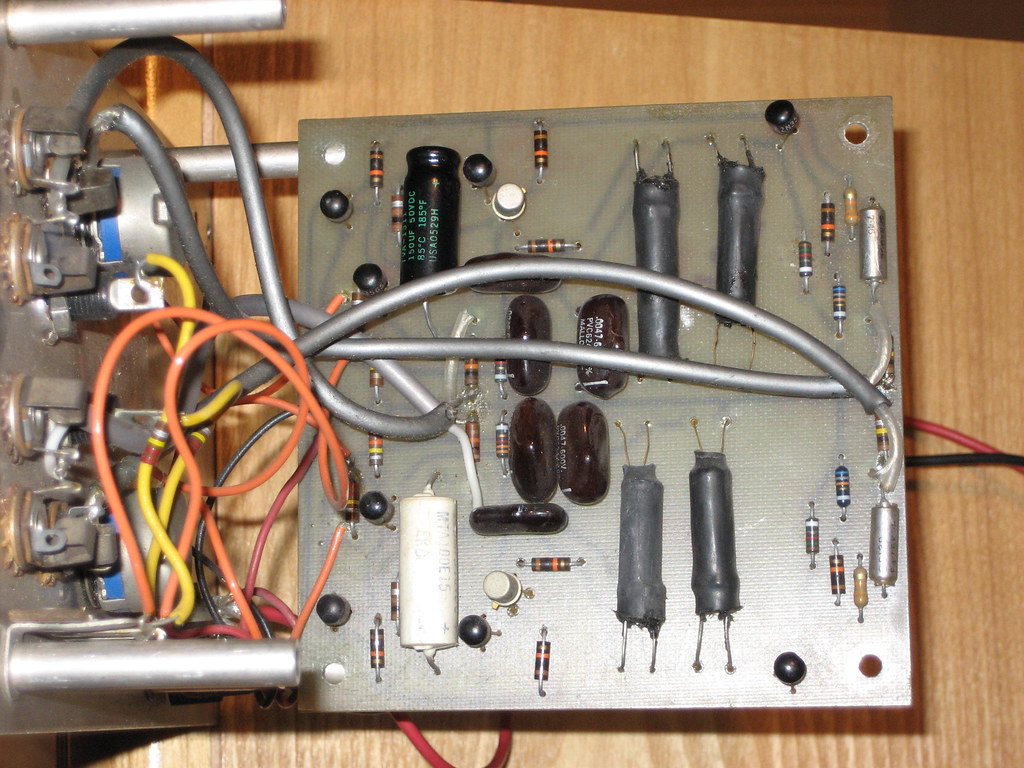
Prototype PCB, no Reverb send:
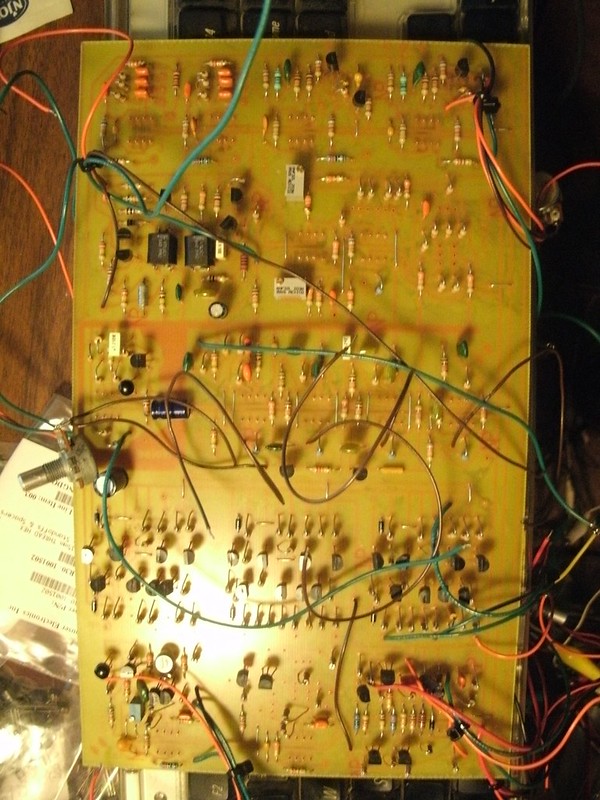
I got things reversed and the ICs all mount on the solder/trace side of the PCB:
COMPONENTS:
This build can apparently be done with standard 2N3904 and 2N3906 transistors (I used the indicated 2N3565 where specified and 2N3906 in the majority of places specifying 2N4248 on my prototype and it's just fine). I've provided a 5mm lead pitch for many capacitors so you can use tiny "box" film caps for the many 0.47uF types found here as well as other values.
A few Tantalum capacitors appear here, 4.7, 2.2, and 1.0. Some are used in the audio path.
The Gates specify vintage IT122 or ITE122 dual transistors; I've got a pair of gain/voltage matched 2N3565 there and it's working. (Linear Systems have a replacement for the IT122.) It may be possible to match up a pair of 2N3904 or BC5X0 types to use instead of the IT122.
The Filter apparently used home-wrangled lamp and photoresistor combinations. Still looking into re-creating this. The Filter also uses one rare 2N4339 FET, unselected.
The Preamps also use one unselected 2N4339 per. A J201 FET might work as a substitute.
The Ring Modulator is the exception, requiring a pair of rare 2N4341 FETs, matched to -1.35V at Vss and a Voff characteristic between 3.0 and 6.0 as well, and a pair of 2N4916 which would appear to benefit from matching; not yet certain if it would be for voltage, gain, or both. There are some resistor pairs involved here which might also benefit from matching:
R21/R25 3K3
R20/R26 33K
R19/R27 33K
R11/R12 680K
R9/R10 150K
Although they're not specified for matching it may benefit the circuit. 1% type resistors should be plenty.
There are some resistor pairs in the Gates which might also be useful to match.
Note that apparently not a single resistor in the schematics is specified to be 1%.
910pF caps appear a couple of times; Mouser sell a ceramic 910pf but if you're against that appearing in the signal path (remember this uses 741s so that's pretty much moot), use .001 film types. I don't know if this will cause any sort of perceivable offset in the circuit (FFB).
6mm multi-turn trimpots are specified here but 3/8" types will fit in the RM (not recommended; the 20Ks will bump up a bit on neighboring resistors). 3/8" types will not fit in the Gates.
BOM, subject to possible error:
1) 2.7R, 1/2W
6) 10R
3) 22R
3) 47R
3) 100R
1) 150R in Envelope Detector?
17) 220R
12) 330R
3) 1K
4) 2K2
8) 3K3
3) 4K7
10) 6K8
23) 10K
12) 15K
13) 22K
13) 33K
18) 47K
10) 68K
3) 82K (Fixed Filter Bank)
5) 100K
7) 150K
5) 220K
3) 330K
5) 470K
2) 680K (Ring Modulator, possibly 1%/matched)
4) 1M
3) 6M8 (Envelopes)
2) 10M (Preamps)
8) Diodes: 1N457 Mouser
512-1N457
1) 200uF electrolytic capacitor (220uF okay?)
1) 100uF electrolytic capacitor
1) 10uF electrolytic capacitor (25V or such)
2) 4.7uF tantalum capacitors
1) 2.2uF tantalum capacitors
7) 1uF Tantalum capacitors Mouser 80-T356A105M035AT
14) 0.47uF film capacitors, 5mm pitch lead.
1) 0.1uF film capacitor, 5mm pitch lead.
2) 0.01 film capacitors
5) 0.022uF film capacitors
7) 0.0047uF film capacitors
2) 0.0022uF film capacitors
3) 910pF film or ceramic capacitors (1000pf / .001uF might work fine)
2) 470pF ceramic capacitor
9) 100pF ceramic capacitors (monolithic axial)
23) 2N3565 (2N3904 might work fine, untested)
19) 2N4248 (2N3906 appear to work fine)
3) unselected 2N4339 FETs. J201 might work (untested)
2) selected 2N4341 FETs for Ring Modulator (test procedures unknown). J202 or MPF102 might work; untested
2) selected 2N4916 transistors for Ring Modulator (for Vbe or Hfe, unknown)
2) IT122 dual transistors for Gates (Linear Systems have a direct substitute; pair of matched 2N3904 might be fine)
"PN" prefixes for transistors are fine as "same as" replacements. For example, PN4339, PN3565.
15) 741 opamps. Haven't checked to see if LF351 or TL071 are immediately compatible/improvements. The 100pF caps associated with them might have to be changed if other opamp types are substituted here.
2) 20K 6mm multi-turn trimpots Mouser 858-64YR20KLF
2) 5K 6mm multi-turn trimpots Mouser 858-64YR5KLF
2) 100R 6mm multi-turn trimpots
1) 1K 6mm multi-turn trimpot Mouser 858-64YR1KLF
The Gates also utilize the IT122 dual transistor found in the 100 series. Two are required here. Linear Systems make a replacement (same name). It may be possible to use a pair of matched 2N3904 etc. for this.
DIY PCB:
The good news is all of the modules listed fit comfortably on a 5.91" X 11.81" PCB. If you use one slightly smaller the Reverb send doesn't fit but the rest does. This smaller size is what you see in the above photo of the PCB I etched as a prototype to test. The Reverb driver and Audio Power Amps are on separate PCBs (in the power supply case in the original).
I've worked these out so that you can cut-and-paste sections of the PCB art if you only want to build certain sections (or multiples) on 6" X 4" PCBs which fit behind single-space Buchla panels.
Being large, this might pose slight problems in exposure and etching. I use two long "neon tube" exposure lamps so an 8-minute exposure was plenty, and etching it in a Pyrex tray with unheated, uncirculated Ferric Chloride took about an hour. The traces are fat and the text is large so it's not exceptionally prone to over-etching errors. Note that a long piece of glass or two medium pieces are required to hold the art flat during exposure. Edges can curl and cause problems in the exposure.
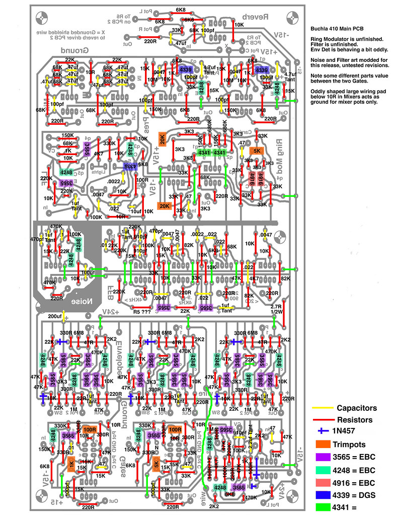
PCB ARTWORK:
You'll note in the prototype photo above there are no ICs visible. That's because I screwed up and they have to be mounted on the trace side of the PCB. Works fine, however. D'oh. >_<
Optimized for pre-sensitized positive photoresist PCBs.
electro-music.com/forum/download.php?id=36040
or visit here to download directly:
http://electro-music.com/forum/viewtopic.php?t=60025
You will note that I've messed up while drawing the art...the ICs have to be installed on the trace side of the PCB, not the parts side. This is easy if you don't use sockets, but sockets are recommended. Mil Max machined pin types are useful here as there is some leg exposed for soldering to pads.
AFTER ETCHING, CHECK CONTINUITY:
Click the pic to get to a "download original size" option. Mmm, colors...
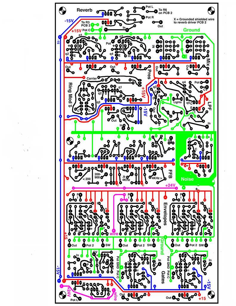
JUMPERS:
After making sure there are no bridged traces, install the Jumper wiring and the single jumper wire (+24V "WIRE" pads are connected across either side of the board with an insulated wire. Recommending that you install the wire on the parts side because on the trace/solder side it would impede defluxing.). Jumpers and the jumper wire are bright green.
High-resolution PDF of this graphic:
electro-music.com/forum/download.php?id=36041
REMEMBER: THESE SECTIONS DO NOT YET WORK: FILTER, ENVELOPE DETECTOR, RING MODULATOR, NOISE, GATES
OVERVIEWS
FILTER:
Currently (no pun) non-functional. I found I'd left out a 10R resistor in the ground path on my first etch. This artwork corrects for that, hopefully as intended. I have not etched it to see.
The filter is evidently similar to or from the 192, in that lamps and photoresistors are used to control the circuit in response to voltage (the 192 evidently was only connected to a pot providing voltage but could then be easily modded to allow external CV control, much in the same manner the 158's waveform control may be IIRC, and here as well as the envelope Attack stage responds to a pot's voltage).
Buchla 192 via buchlajoe on Flickr.
I have a pair of 5C1 Vactrols in the circuit for testing purposes and the Frequency control sweeps it across some of its range, does not open all the way.
If the Mixers are inverting, a feedback loop could be set up which should excite some resonance. A Preamp in the path might force enough level if a Mixer alone cannot.
GATES:
An opamp variant of the 110. THERE ARE VARIATIONS ON PARTS VALUES BETWEEN THE TWO GATES. MAKE SURE YOU CHECK THIS. The Gates also each have a 10R between system ground and their ground path. Don't wire Gate pot ground to system ground; a pad is provided for this isolated ground to the level pot.
ENVELOPE DETECTOR:
I'm not certain this is working correctly. The CV out sits at about -3V when not triggered. The fault of what I thought the schematic said was a 150R resistor, and it should be 150K?
ENVELOPES:
I've got 2N3565 and 2N3906 working side-by-side just fine. 15V output!
Later Buchla envelopes improved the one-shot/sustained circuit through the addition of a diode.
Envelope power is isolated by a 2.7R 1/2W carbon composition resistor. A single wiring pad, next to the word ENVELOPES on the PCB trace side is run to the appropriate Envelope pots for power.
I note that the Decay section is controlled by 0-15V from the pot. This means voltage control, even if it's only of decay, should be as easy as adding a banana jack and some small resistor to the pot lug going to the circuit. (Some 100 series modules added VC to functions in exactly this manner; no mixing of CV signals, etc.)
NOISE:
Found an error in my prototype PCB, corrected here but untested.
MIXERS:
Haven't tested them. Will produce a wiring document as this section has its own ground for use with the pots.
Note there is an isolated ground path on these; a single pad with lines coming from it should be wired to the grounds of all Mixer front panel pots.
PREAMPS:
Working fine.
FIXED FILTER BANK:
Working fine, aside from R5 being unknown.
WIRING:
Will post some instructions here shortly (no pun intended yet apparently unavoidable).
GATES
Have their own ground to the potentiometers; wire the "Pot GND" pad in each Gate to each Gate's pot. "Pot C" nearby go to each Gate's pot center lug. Audio in goes to the other. The pot apparently merely attenuates the input signal and does not provide an initial level for the Gate. CV is required to open them.
The In solder pad is CV in.
MIXERS
Have their own ground to potentiometers; wire from the large pad with the lines coming from it to a single Mixer pot ground and chain that out to the rest for both Mixers.
ENVELOPES
Each Envelope's P1 pad on the top of the Envelope art goes to the right two lugs (top view) of the 250K linear pot. This is the Attack pot.
Ground for these three Attack pots is provided in the Noise ground plane directly next to the left-most Envelope P1 pad. Wire that to the left pot lug and off to the other two left Attack pot lugs.
The center wiring pad on the bottom of the Envelope are labelled "Pot 2". Wire each of these to, top view, the right two lugs of the 50K Audio pots, which are the Decay function.
Next to the word ENVELOPES on the PCB trace side you'll see a wiring pad which provides power to the Decay pots. Wire it to the left lug of one pot and chain it to that lug on the other two Decay pots.
This also suggests that the Decay function is voltage-controlled. It would be desirable to add a CV banana jack with whatever resistor value is appropriate to provide external control to this function.
Switches: The Gate input goes to one pin of an SPST switch. A 0.01 capacitor is wired to both switch lugs. A 100K resistor is wired to the same lug as the Gate in, and this resistor goes to the ground provided on the nearby Attack pots. The lug with only the cap wired to it is then wired to the "SW" pad on the PCB.
The "Out" PCB solder pad obviously connects to the banana jack Envelope output.
ENVELOPE DETECTOR
Add a "sensitivity" control by having the audio in go to one side of a pot, the center to the PCB audio input, and the other outer lug to ground.
Next: The reverb and audio power amplifier circuits.