This page is a work in progress and will be updated as is possible. It is possible I've gotten things wrong as I'm writing this between builds and not during while the info is fresh in my head.
I emailed Don in 2011 requesting permission to make public this new artwork, slightly modified, of his 258B dual oscillator design, and heard back from an assistant, with no specific answer ever given.
This is a serious project, not for beginners.
Repeat: This is a Non-Trivial build!
This can also be a howling pain in the ass. If you build it, you cannot expect me to have any answers for you in regard to trouble-shooting as the circuit is far beyond my understanding. Seriously; you're on your own.
Will shortly upload etch artwork, parts layout, schematics, etc. Leaving this here beforehand so you'll have some understanding of what you're putting yourself into.
The J3RK clones are far friendlier builds, have linear FM and track at 1V/Octave! Roman's clone is even better because it eliminates the need for pain in the ass front panel wiring!
Sourcing the rare parts in this build can be a major factor in whether or not you can actually finish one once you've gotten started! If you've never etched a 2-sided PCB you may not wish to start here! Desoldering can ruin pads and traces so be very careful!
Note that I am not a tech and have run into trouble-shooting issues with this build, and they are above my head. This circuit is beyond my knowledge of circuitry (which is nearly none). You will not get any help from me if your build doesn't work beyond everything I have posted here. I just don't know. I'm a sound designer and a strong Buchla enthusiast who needed to see this design happen but that's all. Build at your own risk. Have a good tech lined up...
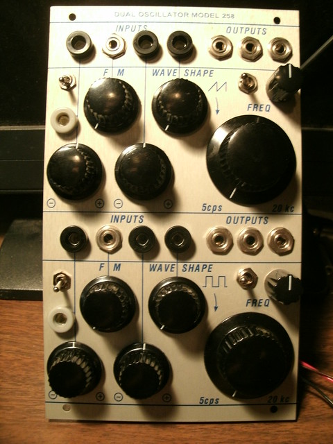
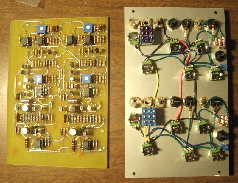
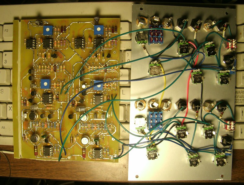
The PCB was not designed with the original front panel layout and hardware in mind. This version fits behind a panel via three standoffs epoxied to the panel, with the parts on the outside, which is not optimum. This is if you are using Alpha 16mm pots. With 9mms there may be enough room to flip over the PCB and find empty places on the panel correlating with empty spaces already in existence on the PCB.
It is recommended to tin the PCB with solder after tinning it with something like Liquid Tin.
Two things which Don Buchla did which are not provided for in this build:
1. The timing capacitor should contact as closely as possible the 3565 transistor pair. J3RK's clone PCBs address this. Use an axial cap, the Mouser part # 23PS247 instead of its radial version, and solder a short lead on one side to the end trace near the trannies. The other lead can be long to the original solder pad.
2. The FET which is trimmed (1M) for sine purity should pretty much directly contact the trimpot lead itself instead of the inch or so of board trace involved. Mount the trimpot high enough off of the PCB to solder the lower left leg to the circuit board top trace pad and have the upper leg bent out to connect the middle FET leg directly to the trimpot leg.
FEATURES DIFFERING FROM THE ORIGINAL
-Switching between Saw and Square per oscillator
This design has an addition thanks to L-1. Years ago on EM he posited that Don's original design, which offered a square wave on one oscillator and a saw on the other, supports the possible use of a 3PDT switch to select between either saw or square per oscillator, if all of the parts were designed in to a single oscillator. I've had that done so here. Thank you to L-1! You will find that J3RK's clone also uses this wonderful feature. In this design as well, jumpers may be used to select only one waveform per oscillator instead of wiring up a switch.
-Triangle waveform output
If desired, you can wire this output to one or more of the three (typical) output jacks. I wire mine to have the first one triangle and the second two, the sine/variable waveform.
-FM Switch
This is wired at the front panel. Basically, a DPDT switch to go between the factory plan of input-> 1uF tantalum cap ->33K resistor -> amount pot and a straight wire. The straight wire path allows for extreme exponential audio-rate FM resulting in an expansion of the units timbral range. Recommended, but you certainly don't have to do both if you choose.
-TEMPCO mod
The originals utilized a 2K 1% metal film resistor where a TEMPCO may also be placed, but the originals were decently stable. A fella, a clever fella, might just use a switch to select between "Vintaj" and "TEMPCO" behaviors. Using a modern power supply on these might make such moot.
-Limited 1V/Octave tracking
It's possible to have the additional banana jack (gray in the above image) connect to a tiny 200K multi-turn trimmer and then to the appropriate CV rail. Can't promise much tracking from this design but some might be interesting.
COMPONENTS
This build involves some frighteningly scarce components. Even some of the substitutes are scarce. Not for the beginner!
RESISTORS
5% carbon film resistors are recommended excepting those indicated at 1% and the carbon composition types.
Don specified carbon composition resistors in his original schematic for certain value multipliers (1, 2.2, etc. meaning 2.2R, 2K2, 10R, 1K, 10K, 10M). I do not know if this is because he preferred them or if he had a ton of them purchased in bulk, or if they were less expensive in those days than other types. By the time he produced the 258C, there were less CC used. You may if you wish search such out but be aware that some of the ones I've purchased have higher values than stated, at times to enough of an extent that it becomes worrisome. I've used pairs of 470R in series to create CC 1K resistors for one place, for example. There may or may not be an audible difference when they are used at the output section (both saw and square have CC resistors). See the original 258B schematic for Don's notes.
I have taken to using Kamaya and other modern brands of carbon composition resistors for these builds due to them being closer to the original values (especially one of the 1Ks which must be selected for 1% tolerance). Available at Mouser, etc.
Several odd 1% resistor values are present. Some appear to require matched pairs. The schematics do not mention needing them to be matched. It is up to you.
The sine shaper section appears to require 1% or better matched pairs of resistors (330K and 680R) as well as a pair of 1N457 diodes. The schematic does not mention 1% or matching. It is up to you.
OPAMPS
There are only LM741 opamps in this. If you wish, you may experiment with using something more accurate and modern for the control section and the audio output section. I have not. An LF351 would be a great bet; I like the sound of those better than the TL07X. Hopefully it will work as you will get snazzier highs and a cleaner midrange. A discrete output section would sound best! However, when you get into the exponential audio-rate FM possible on this device, and its pitched noise chaos, you may be glad that the high end is a tad tapered by an old opamp. You may wish to change only the output opamps. Socket them, however; I haven't tried swapping them out so I don't know if they'll work in this specific circuit.
Update: I'm told the 071 will swap out with no mods required except for the Waveform circuit where a 10K resistor is used for stability; the 071 does not require the stabilization so remove the resistor if you wish to use an 071 therein.
TRANSISTORS
There are two matched pairs of 2N3565 (or PN3565) in each oscillator. I have no idea if they need to be matched for gain or voltage or both, in each or either place. One pair is at the timing cap; the other is part of the squaring section for the square wave, IIRC. I am told that voltage (Vbe) matching is all that is required for both pairs.
A 2N4341 is used in the waveshaping section. This part may not be critical, or a substitution may effect the saw/square character. I don't know. J3RK's clone works just fine with a substitute; MPF102, I believe.
The sine shaper JFET is trickier. A 2N4339 must be selected for an Idss of between .8 and 1.1 or so. 0.7 to 1.2 might be acceptable; I haven't tried. However, on my J3RK clones, a selected J201 sounds very different when out-of-range. I have not done a swap to compare how they sound when calibrated, if there is any difference. It's up to you. Purchase enough of either J201 or 2N4339 to allow one or two of them to show up in the desired Idss range. (J201 max out at 1.0 Idss, and out of many I've purchased, none measured above .90.)
BUILD CONSIDERATIONS
Audio output levels are 1.1VRMS, which is +4dBu and below that which is used in more recent systems from other manufacturers. From what I'm reading online, the 200e oscillators have an even lower output level (and the 100 series evidently do as well).
Power is +/-15V. The CV range on the waveshaper input is about 15V, and with stock input CV resistors on the pitch section, it's about 2.0V/Octave, so this is designed for use within a Buchla system, where sufficient CV ranges exist to fully sweep the pitch and waveshaper throughout their ranges.
Power decoupling caps (.1uf ceramic) were added into this build. They are not present in the original. Some of them act as vias for ground and voltage rails so please install them. If you completely reject them, make certain that you solder in a lead wherever a via is required to carry the rails between sides of the PCB.
Two resistors (R15, R18) are used for tracking calibration instead of trimpots; these resistors can be 5% per the original or 1% or even more tightly matched if you wish. I imagine that making R12, R17, R19, and R20 1% would "help" as well. And would also take you further from what the original.
I use #65 drillbits. This is perfect for ICs, resistors/capacitors/diodes etc. as well as for wiring, so long as you use 24 gauge wire. Note that the 2.2R 1/2W resistors require a larger hole.
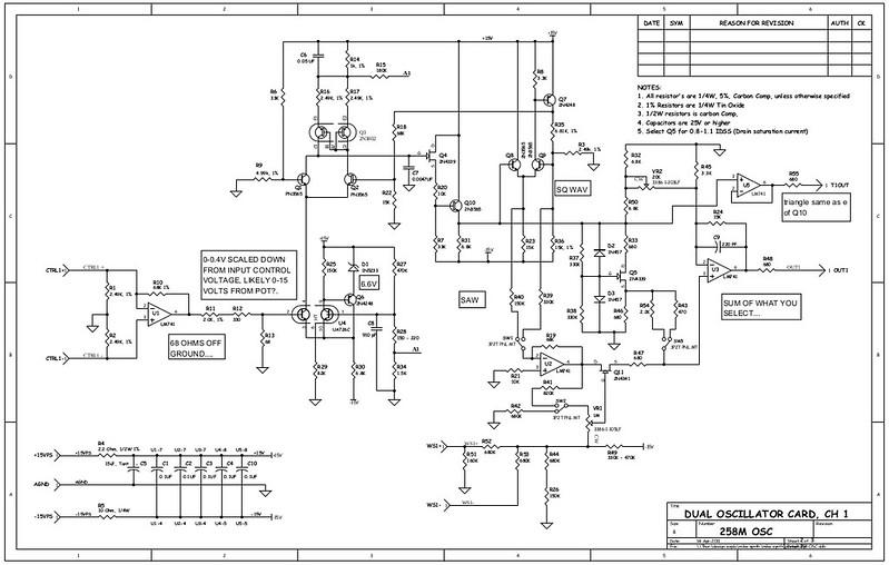
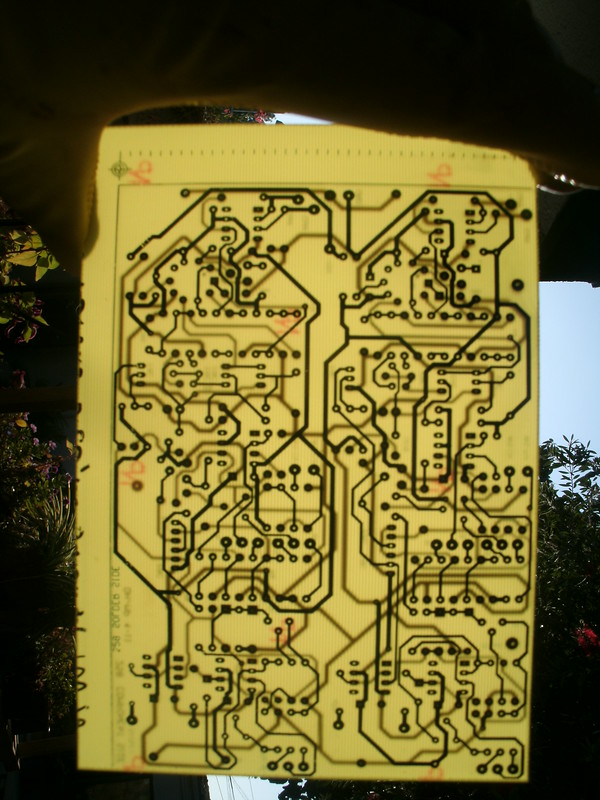
This does not include the front panel wiring. Click here for a larger version:
http://electro-music.com/forum/download.php?id=36291
Permission is not granted to use this for commercial interests.
EXPOSING AND ETCHING TWO-SIDED PCBS
Double-sided is a bit tricky when lots of ICs are involved; you have to get the pads just right. I peel one side of a double-sided board, tape down the artwork, and under a "bug light" drill through two significant pads on each end (diagonal) of the board, through the artwork. Peel side two and align the art with the holes (press down the material first, flattening any material raised by the drilling) and tape it down. Expose, etc. I always allow one pair of sides (side and board bottom) to be the natural boundaries/edges. One trick which helps is to have text on each transparency saying which side is the TOP and which is the BOTTOM, and the text will be the "key". If you can read the "top" and "bottom" text you've written on both sides when they're on the PCB, you're good.
It is very important to check the top-to-bottom through continuity on the integrated circuit sockets (machined type are recommended here). Use a Voltmeter set to diode or a beeping continuity tester to check. In some places the IC pins are used as bottom-to-top etc. power and ground throughput so you can get into trouble here. Will update with an image of the pins and points to be checked.
And hella beware the thin traces. They can easily etch too far and leave nearly invisible breaks. A single hair on the transparency or upon the glass flattening it to the board, unnoticed, can cause full breaks in traces. Continuity testing is an extremely good idea, from solder pad to solder pad, and up onto the legs of transistors above solder pads, once installed.
Dr. Stinchcombe examined this circuit and two of my builds and found the micro-breaks in the thin traces. Continuity testing is imperative as is hand-soldering in heavier tinning than Liquid Tin provides. (Add solder after Liquid Tin has set.) This is also absolutely no guarantee that a complete break may occur even when traces are tinned with solder. I've found one through holding the PCB up to the light so be careful. That's Tim's idea; thank you!
On my most recent built, I somehow managed to use the tongs with which I lift PCBs from the etchant to rub across the front of one while in the etching tray; had to repair several broken traces with resistor lead clippings across them.
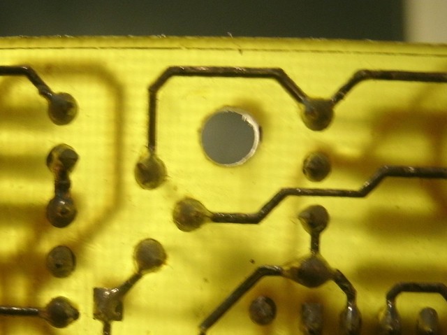
Micro-break from exposure / etching, not visible to the naked eye. This is =after= having tinned the traces with solder. It didn't jump the break and just barely did on the right. This is the +15V trace; it reads +15V above the break, and +4.35V below. Inexplicable until you hold the PCB up to a strong light. Thanks to Dr. Stinchcombe for that trick! Positive expose PCB development is vulnerable to such issues. I've never attempted two-sided press and peel.

When I etch and tin, I use thick rubber gloves such as these because thin ones don't appear to repel etchant, alcohol, acetone, and liquid tin. However, I cannot say whether I'm supposed to feel loving, or feel loved, when using these gloves. I call shenannigans!
DRILLING
Drill the bottom side first. I use a piece of notebook paper on the drill plate with the PCB on top of it so the traces don't become scratched.
Hundreds of holes. The Vias are easy to overlook if the etch didn't go deeply enough to reveal the drill hole guide.
After drilling, hold the PCB up to a strong light to see if any undrilled pads remain.
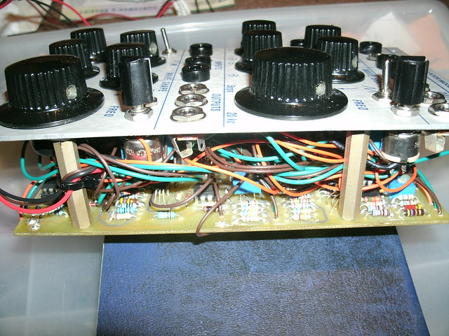
Some parts are flown across the front panel wiring and pots. This is indicated in the original schematic on its left side.
PARTS
Some parts specified are of "loose" tolerance and it is possible to use ones with less variance, but you may lose some of what makes the module interesting. For instance, 1N457 diodes are specified but you can use 1N457A, as well as ignoring the 1N5233 and using an A or B version (each being tighter tolerance than the previous). Very few 1% resistors are specified in this build; indeed, the carbon composition excepting the 1K are all at a 10% tolerance. If you are the sort of person this pisses off for whatever reason, you can use all 1% metal film resistors in this build if you must.
Diodes are Fairchild 1N457A, 0.17 cents each at Mouser (went up 7 cents in recent years) :
http://tinyurl.com/5wowafm
The "A" version is a cent less expensive than the specified 1N457.
Cheapest PN3565 source is Tayda, at .10 each. There is no mention of a price break for quantity.
http://www.taydaelectronics.com/t-transistors/pn-series/pn3565-2n3565-3565-npn-transistor.html
Mouser have PN3565 but they're currently 0.58 each (610-PN3565).
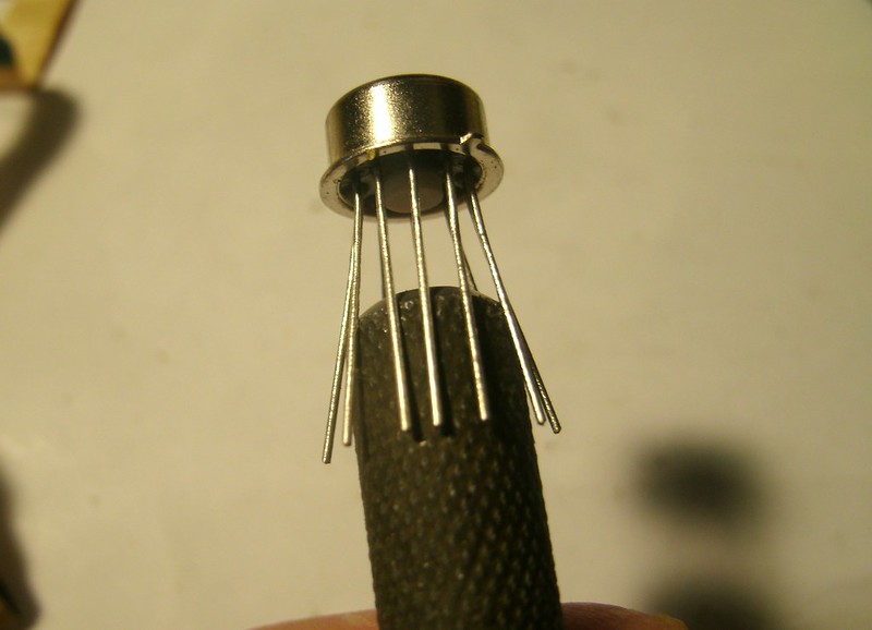
Motorola 2N3802 were used in this design; other 3802s may have different pintouts and must be twisted into place accordingly. Indeed; I've come across Motorola 3802 in different metal can sizes/types and the pinout is different. Sigh...
uA726, two per board, may be purchased from various Chinese sources. Caveat emptor.
One Zener diode, a 1N5233, is used per oscillator. There are versions with tighter tolerance: 1N5233A, and even tighter, 1N52323B.
SUBSTITUTIONS
J201 for Sine Shaper FET. You must again select it for .80 minimum Idss. Less than .7 will likely result in a buzzy sine wave. Again, the pin-out is imperative. Soldering it in without correct GDS orientation will produce zero or undesired results.
1N4148 may be used instead of 1N457 but you'll make me sad if you do. ;)
You can try 2N390X types for 2N3565 and 2N4248 but I don't know if they'll work. Update: Have used 2N3906 in place of 2N4248 and confirm they work, but haven't done more than check for oscillation and pitch range so I'm not sure if they compromise anything in actual use. (Since posting this I've used 2N3906 in place of 2N4248 and there appears in initial testing to be no difference. Mind you this is only at the level of powering up and confirming oscillation.)
2N550C/560C for uA726 and 2N3802. Will drift a lot.
Linear Systems LS132 substitutes for 2N3802. Note the pinout on the PCB and check both sides of the 132; correct accordingly by twisting around the component legs.
If you absolutely cannot find 2N3802 and uA726, make sure to have each pair of resistors face-to-face and treated with a touch of heat transfer grease. The 2N3802 Motorola pinout/footprint is what I used for this layout and it allows discrete transistor pairs to face each other. I believe I've once tried this with the uA726 and it is also possible there...
MATCHING
-The two pair of 2N3565 or PN3565 per oscillator may be matched for voltage (Vbe) to 1% or greater. I have no idea if the originals were or not. Matching is easy and is a very good idea in this case; I have heard of one clone maker (not Verbos) who experienced a very weird response curve to voltage until he replaced the first pair with a matched (Vbe) set.
-The 330K, 680R, and 1N457 pairs in each sine shaper section may be matched as well as you wish, but you might lose some of the variance which makes things interesting.
If you've never matched diodes, many VOMs have a Diode test setting. Do not touch the diodes; use a needle-nosed pliers to select and move them. Heat will change the reading as it dissipates so don't touch them. With a diode in front of you, touch the VOM test leads to the diode legs. If there is no reading, change sides and note the correct leads. You should see a reading such as "630" or similar. Select two diodes with the same number for a 1% or better match. Diodes differing by one or two last digits are absolutely acceptable because that's only two or three percent variance. I have no idea if the original had matched diodes and resistors in the sine shaper so "no worries".
SELECTING FETS FOR IDSS
The sine shaper section requires one selected FET per oscillator, two per board.
Determine what brand of FET (2N4339 / PN4339 or J201) you have. Download the datasheet which will tell you the pinout. If you don't know the manufacturer and pinout of your FETs, you can use the same procedure to swap between them until you see a reading. You may burn up a part or two to determine the correct pinout.
http://www.forsselltech.com/media/attachments/JFET_Jig1.pdf
You only need to test for Idss, so the entire bottom section may be ignored. This may be accomplished with alligator clip leads to a 9V battery, the FET, and a VOM.
-Connect the battery positive to your AC current meter's positive/red test lead.
-Connect the ground/black test lead to the Drain ("D") pin of your FET.
-Connect the battery negative to both the S and G pins of your FET (one alligator clip will suffice).
-Set your meter to read the correct amount; 2N4339 should range from about 0.5 to 1.5 or so. J201 will read from less than 0.5 up to 1.0, but in a bag of several dozen I once purchased, only a few reached the 0.9 range and none occurred in the upper 0.9s or even 1.0.
TEMPCO mod
The originals utilized a 2K 1% metal film resistor where a TEMPCO may also be placed, but the originals were decently stable. A fella, a clever fella, might just use a switch to select between "Vintaj" and "TEMPCO" behaviors. Using a modern power supply on these might make such moot.
BUILDING IT
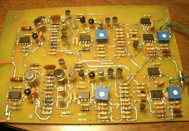
Fully-stuffed PCB; still needing to be cut to size.
After exposing the PCB/art, develop it and check with magnifying glasses for any breaks due to hairs on the glass or transparency, etc. Fill in with a Sharpie permanent marker or similar. Etch...
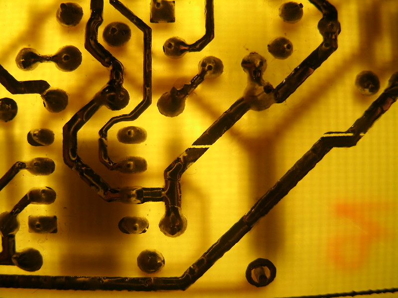
Just-etched PCB. Note the breaks on the dark, downward-going trace at the upper left near the pad. When the resist breaks, the etchant eats what's beneath it!
After etching, cutting the PCB to size, and tinning the traces, hold it up to a strong light and with magnifying reading glasses, check the visual continuity of all traces on both sides. If there are any gaps in a trace, use a clipped resistor leg to jumper them in place. (The same goes if you ruin a pad while desoldering; use a clipping to extend the trace to the component.)
-Use a meter set to diode mode to check the continuity of traces, that they work from point-to-point.
-Check for shorts between traces if they didn't etch deeply enough. Separate them with repeated cuts from a blade until they read as disconnected.
-Vias
There are several vias which must be through-connected using resistor or transistor legs. Do these first. A clipped resistor leg works fine; bend them over a few millimeters and solder in; then clip and bend the other side's remaining lead along the trace connected to the Via, soldering it in.
(PICTURE OF VIA LOCATIONS)
I recommend de-fluxing the top (parts) side of this build in stages, as there are some tight fits making it difficult to do so after all components have been mounted. This is also why tinning the PCB with solder after using Liquid Tin is a very good idea; repeat de-fluxing may begin to remove some Liquid Tin. This is one of the big issues with this build; soldering on the top side can result in difficult or impossible cleaning/defluxing.
Bypass capacitors (0.1uF ceramic) (deflux)
2N4248 in uA726 section (deflux)
uA726 (push pins apart with Xacto) (deflux)
uA726...I use the end of my Xacto knife to spread the legs out to accommodate the PCB pitch.
PCB orientation: Note that the tab on the uA726 denotes pin 10, not pin 1. Pin 1 is directly to its right. The square pad on the PCB denotes pin 1, and in the center of the ring is text stating "TAB" with a marker to the appropriate hole.
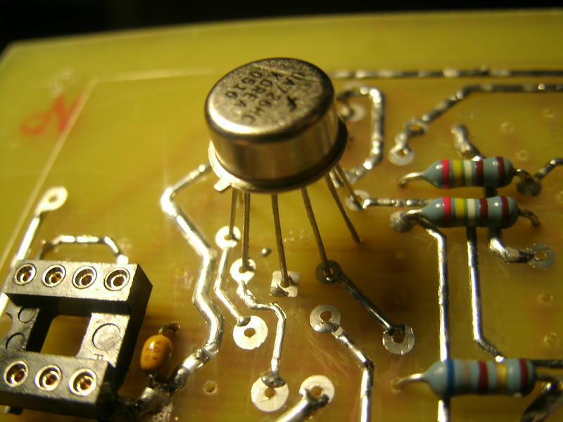
Note to solder it first, deflux, then surrounding components.
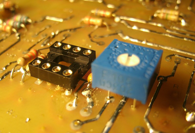
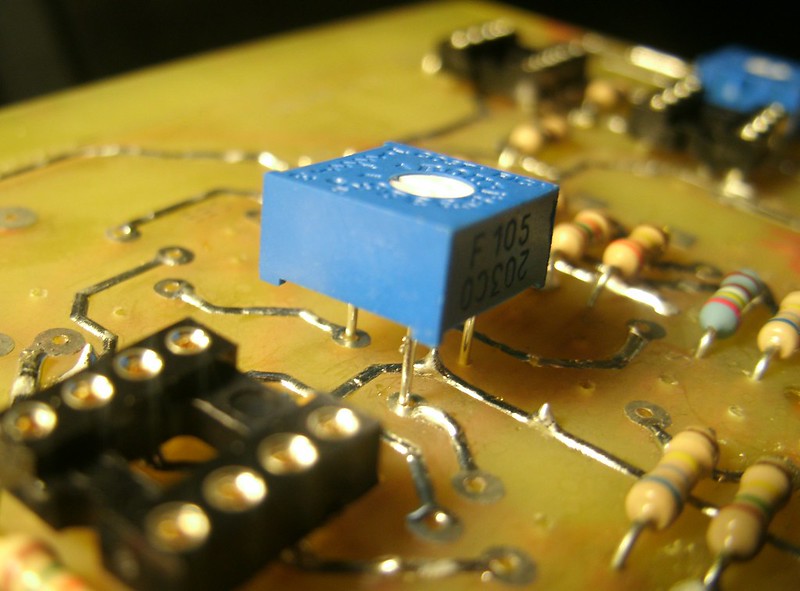
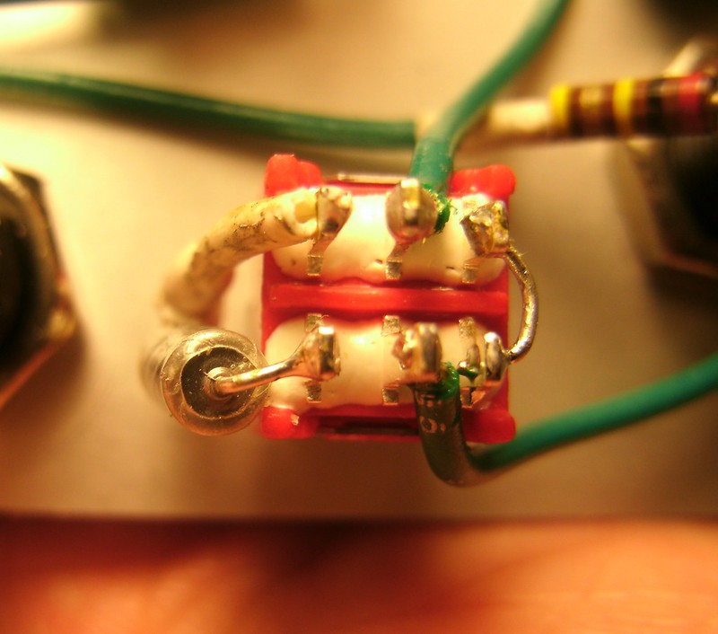
1M trimpot. You'll want this as high off the PCB as possible due to legs needing to be soldered to traces on the top side of the PCB. (deflux)
1M trimmer installation. Solder them before any directly surrounding components.
Solder them as high off the PCB as you can, meaning with only a tiny amount of lead showing through on the solder side:
This will leave space beneath the trimmer to solder the legs to the appropriate top-side traces. One on the bottom trimmer, two on the top. Then deflux the top side!
680R and 220PF capacitors in the sine output section (deflux)
Integrated circuits (solder to board or use MilMax high-reliability sockets with legs exposed to solder to top side of PCB traces/pads. (deflux)
Resistors. (deflux)
2N3802. (deflux)
Capacitors and diodes. (deflux)
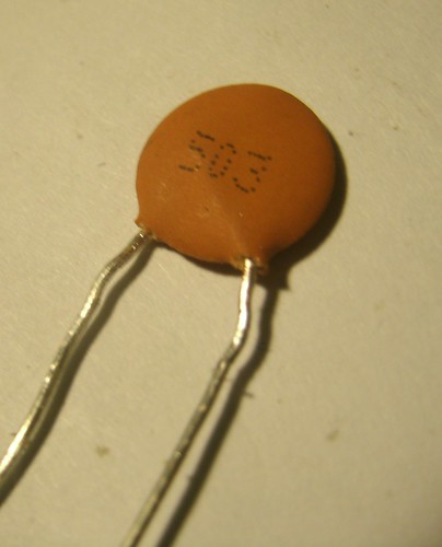
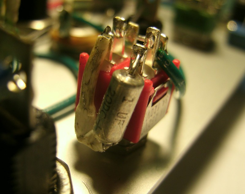
Timing capacitors: you can use axial or radial here but both must be mounted high off of the board (a few millimeters or more) to allow soldering to the pads on the top side of the PCB. (deflux)
Transistors.
Anything remaining except for FETs (20K trimpot, etc.)
FETs.
.05 ceramic disc capacitor. Remove ceramic from legs as both of them are soldered to top-of-board traces.
Deflux!
Now, jumper the following pads to "program" it to produce sawtooth waves for both oscillators. This is for the Testing phase.
(IMAGE)
TESTING
Note the alternate waveform pads (Saw, center/return, Square), three sets per oscillator. Using clipped resistor or other leads, solder across/connect each of the center/return pads to the Saw pad.
PHOTO OF CONNECTIONS TO MAKE
Hook up +/-15V and ground.
Connect audio (grounded to the board/power supply) to one of the sine outputs.
Power up with a finger upon one of the opamps. If it doesn't begin overheating or smoking you're doing well thus far.
If it's functioning, it will be oscillating at around 5Hz. Turn the 1M trimpot until you hear a few ticks a second.
Repeat for the other side.
This will mean that both are oscillating, at minimum.
If you are having a problem at this point, jump to the trouble-shooting section. If things are working as indicated, do the following.
-Wire a 10K pot with one side to ground, the other side to -15V, and the center to a 100K 1% resistor to the "+" CV input of one of the oscillators.
-Check audio at the triangle output. Grounding a headphone and touching the jack to the 680R should be enough to confirm oscillation and a sweep across the entire frequency range. It should sweep from below audibility to above, silent (to our hearing range) at both ends of the pot's range.
-Check audio at the sine output. It might be buzzy pending calibration; not a worry yet.
If it oscillates and responds to the frequency pot from extremely low to above audibility, congratulations! Now calibrate it:
CALIBRATION
There is no calibration for tracking/high frequency adjustment. Those two trimmers were replaced by R15 and R18. You can use 1% or better resistors in those locations if you wish.
-Turn the 1M trimpot and confirm you will hear a strong sawtooth wave, equal in volume to the sine it is mixed in with. Now set it to just over where the saw wave is silent, no buzzing.
-Connect a lead to +15V and touch it to each of the two Waveform CV input pads. Each should instantly produce a full-volume saw wave and instantly turn off (leaving only the sine) when the voltage is withdrawn.
-Re-apply the +15V to either pad and set the frequency control to minimum. You should hear ticking at right about 5Hz (five times/ticks per second) with the temporary frequency pot set to minimum.
-Sine distortion. The 20K pot should be set to where you hear the least amount of buzz in the sine wave, or for the relative "best" sine-like waveform on a scope. Don't expect perfect (this is part of what is good about this oscillator).
DETERMINE WHAT YOU WANT TO DO WITH THE ALTERNATE WAVEFORMS
You can use clipped resistor leads to jumper set either sine or square wave per oscillator. Meaning of course that you can have both be saw, or both be square, or have one of each per the original. You can also use a 3PDT switch (On/On) to switch between each per oscillator. This involves using nine wires for each switch.
These switch types are by nature fairly large. The mounting hole is proportionally so. I mount them in the hole usually reserved for the Fine Tune pot and they fit perfectly.
L1's modification of the 258 series to allow selection of Waveform between square and saw.
FRONT PANEL
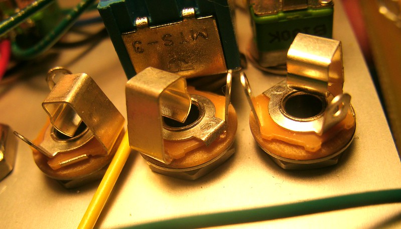
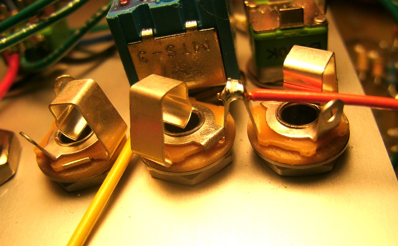
You can use Alpha 16mm pots but it's recommended you get the dust covers available from Mammoth Electronics as they are open (unsealed and vulnerable to dust and dirt). Alpha 9mm pots are also very useful for these builds.
When using 16mm, use a nut on the pot (for behind the panel) and a nut to secure it. When using 9mm, remove the tiny metal nub with a large pliers. Three washers between the pot and the front panel result in a perfect height for the small Davies knobs, just a touch lifted off the front panel when set all the way down the shaft. No rubbing!
The Switchcraft Tinyjax should have a nut on them (between the jack and the front panel) and a washer and a nut on the front side to secure them. This results in the jack shaft being flush with the mounting nut.
A 3/8" nut driver works to secure the Tinyjax. A 10mm nut driver works for the pots.
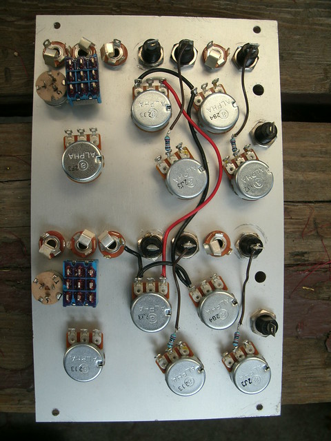
WIRING
Now you're in trouble. Pain, meet Ass.
Have at least five different colors of wire for this project; more if possible. Red is traditionally positive voltage and Black is traditionally ground. Negative voltage can be whatever you wish. Then you'll want at least two colors to represent the front panel's "+" and "-" CV paths which connect to the PCB. An additional color for audio connections is recommended, even having a different color for sine/alt and triangle outputs.
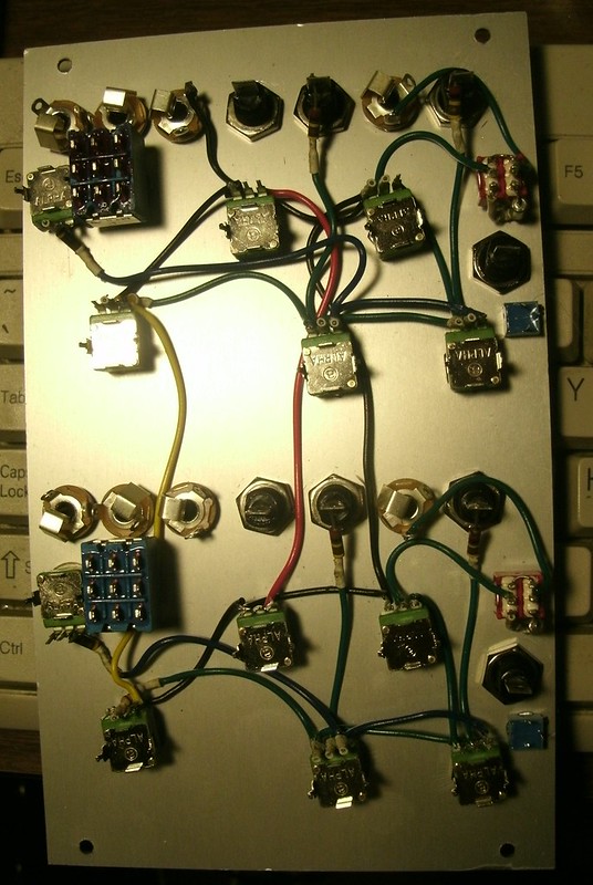
INCREMENTS

Front-panel wiring excepting the extreme FM switch and keyboard input mods. The "keyboard" input banana jack goes where the shown here 10M and 100K pot go on the front panel, which was a fine adjustment for the first Control In path.
Click on the images for larger versions. Click again to get to the "download original size" option for very large versions.
Note that the build depicted eliminates the front panel fine amount trimpot for the left-side CV Amount pot, as is shown in the original schematic. This is useful for fine-tuning keyboard tracking, for example, but an additional mod is theoretically possible using a 200K mini multiturn trimpot hot glued to the panel after a banana jack installed in its place (the banana jack is depicted here).
Using a Rod Serling Fan Club or equivalent front panel...note the large Waveform select switch in the hole where the Fine Tune pot usually lives. The RV6 pot to its left (1/8th" shaft) will be used for Fine Tune, and required a new hole be drilled in the front panel. Alpha 9mm pots are fine here as well but have 1/4" shafts; use a Davies 1900 knob in that case.
Also note holes drilled for the FM switch on the right side.
Ground, + power, and CV inputs. Please use heat-shrink tubing where you see the exposed resistor to wire connections. Ground is also unfinished: it will also be wired to the Frequency pot at the left on its left lug and go up to the RV6 Fine Tune pot as well. Note that ground goes to only a single audio jack's ground lug; this grounds all audio jacks and the front panel together.
This image does not include the ground paths to the Frequency and Fine Tune controls. That's detailed later but may of course be wired now.
I am wiring this version with a triangle output to the right audio out jack; the sine/alternate waveform goes to the left pair. Note that their signal jacks are touching; Buchla did this so I'm following suit. A dab of solder secures them together.
Adding the "+" CV control path (green wires between the Frequency pot, CV Amount pots, and FM Amount pot). Here, two go out from the left CV amount pot to other pots. It's of course possible to daisy chain pot-to-pot instead.
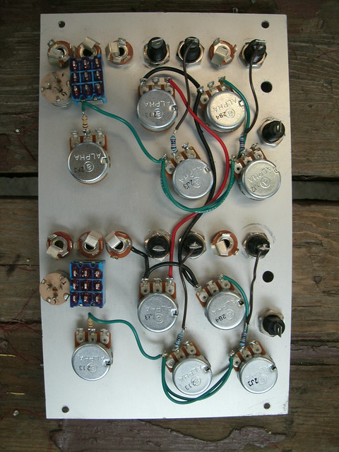
Starting to add the "-" CV control path (orange wires to the CV Amount pots and eventually, to the Fine Tune control)
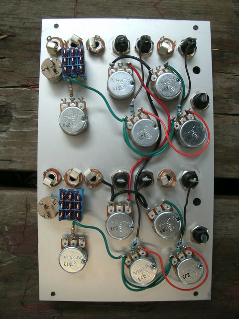
Finishing "+" CV path (orange wires), -voltage (brown wires to Frequency and Fine Tune pots) and ground to Fine Tune pot. Note the 6mm 200K mini multiturn trimpot glued below the additional "keyboard in" banana jack, trim dial facing outward for calibration after the module's completion. Also note the FM switch with both straight wire and (heat-shrink covered)
Here you'll also see the ground connections to the Frequency and Fine Tune pots.
1V/Octave mini trimpots: the pair of 200K 6mm multi-turn trimpots are first set to 107K, then hot glued to the panel, then wired to the banana jack and to the CV rail.
Nearly finished version using Alpha 16mm pots and RV6 pots for the Fine Tune controls.
(Unfinished) version using Alpha 9mm pots. Tricker to solder but you don't need dust covers as with the 16mm pots.
OVERALL PANEL TO PCB WIRING
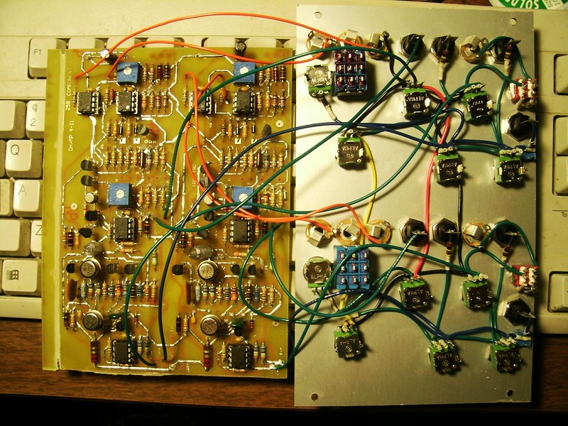
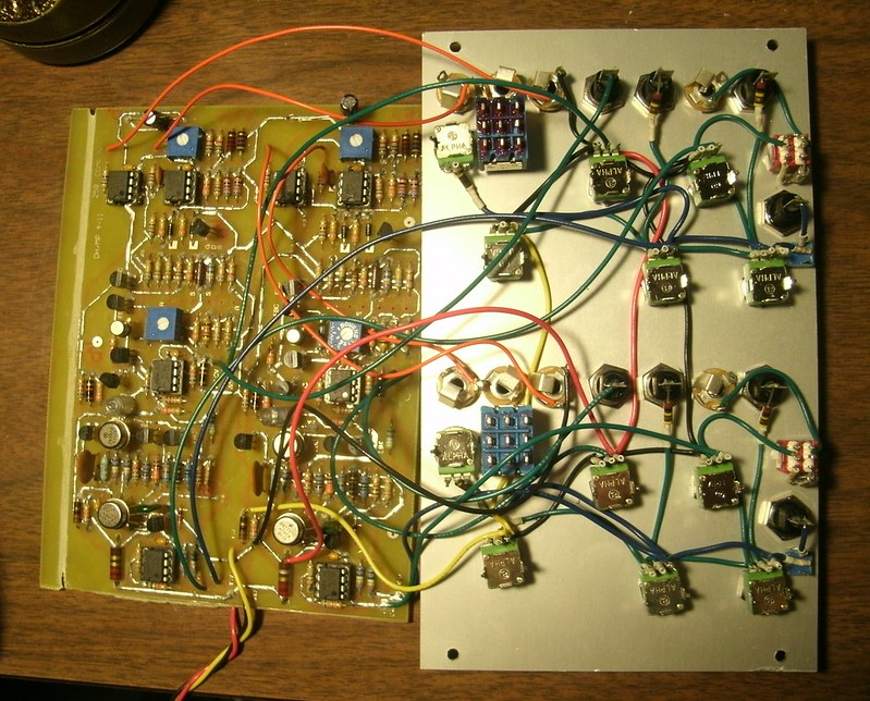
I lay the PCB next to the panel for wiring. This allows the finished version to be "opened" for troubleshooting. This also allows you to determine each wire length by setting it in place from the spool (point-to-point from PCB pad to front panel solder destination) giving it a bit more for slack, and cutting as required.
Set the PCB, parts side up, next to the front panel (knob side down), arranged as such so the three standoffs will align with open space on the panel:
Correct placement. PCB not yet cut to correct size. Power and ground not yet wired to Fine Tune pot. "Keyboard" input trimmer not yet wired.
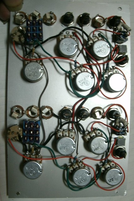
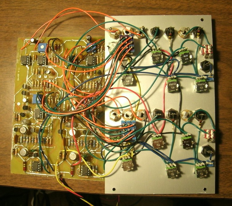
CV paths and Waveform pot and CV inputs wired to PCB.

Extra cat because this is a pain in the ass
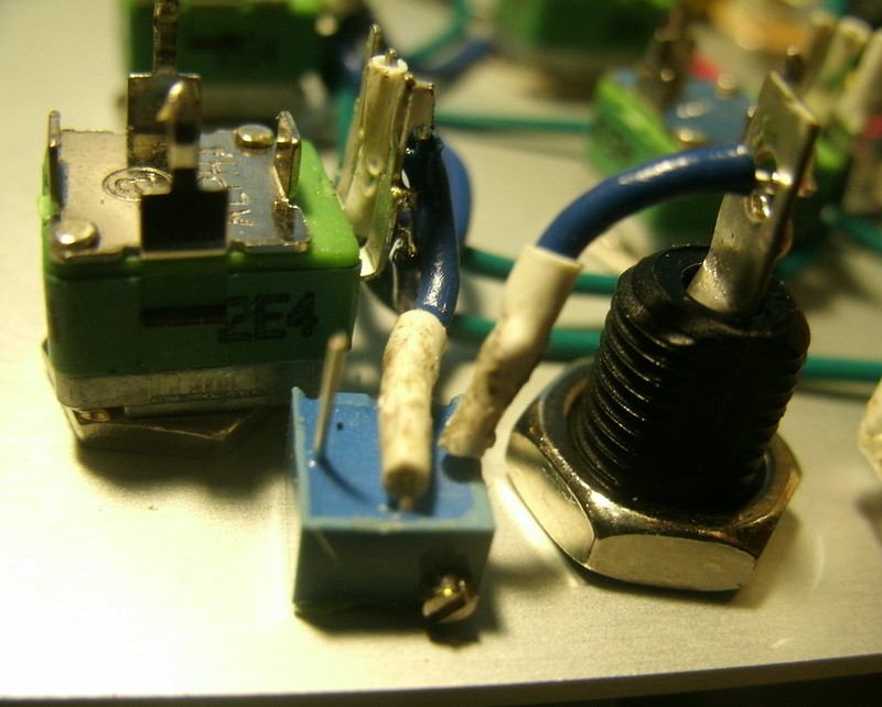
"Keyboard" CV input trimmer wiring.
Hot-glued to the front panel after being set to 107K (untested target for 1V/Octave response), this trimmer is wired to the "-" CV input path. It should be easy to adjust from the sides of the module.
This is Mouser part 81-PV37P204C01B00.
Audio FM path wiring
The original module shows an audio input to a 1uF tantalum capacitor's "-" side, to a 33K resistor, to the "+" CV path. This results in a unique exponential audio-rate frequency modulation effect, which to me is the main interest of this module. Broken robot sounds for days and days, and pitched noise at clever settings (shown to me by Mr. Slater...set both oscillators to 2 to 3 O'Clock (Frequency) with FM Amount on each at about 70%. Patch the sine of one into the FM of two. Patch the sine of two into the FM of one.)
However, this is not the full potential depth. Using a DPDT switch as a router, you may select between the original path and a simple straight wire, a resistor clipping, for full depth. This will cause the oscillator to cease oscillating at certain settings, but adds a desirable new range of tones to the module.
The DPDT's center pins are In and Out connections.
Original path (1uF tantalum into 33K resistor).
Audio Jack Wiring
On original modules featuring pairs of audio output jacks carrying the same signal, Don had the signal tabs touching and ran a wire through them. So long as one audio jack on a module's ground tab is wired to the ground path, the entire panel becomes ground and you do not need to wire any further audio jack grounds.
I wire my builds with the triangle audio output to the left-most audio jack of the three available, with the right two (front panel view) for the sine/alt Waveform.
"High five!" ~Borat
Of course the wire must then be moved out of the center of the jack.
Audio jacks wired. PCB being cut to size. Fine Tune ground and power not yet wired.
Control voltage wiring, audio wiring (orange), and power wiring to the PCB.
I've run +15V from the circuit side of one of the 2.2R resistors to the front panel.
-15V goes from the circuit side of one of the 10R resistors.
Ground goes from the side of the 82K toward the power inputs, to the ground lug of any of the front panel audio jacks.
You can choose several points from which to jumper power and ground from the PCB to the front panel. In the originals, Don used terminal strips screwed to the back of the front panel as the receiving point for power and ground, which then went to the front panel and PCB.
Note: Power to the Fine Tune control goes as such: -15V jumped from the adjacent Frequency pot to the right-most pin; ground to the left.
Alternate Waveform Switching
At this point, you may jumper the alternate Waveforms (hardwired to either saw or square per oscillator) or install the Waveform switches (as seen in the preceding images in what is usually the Fine Tune pot position).
This means 18 more wires.
If you are going to build the Waveform selection switches, please use a different color for each: Square,Ramp (Saw) and Returns.
Board cut to size (not yet sanded) with all power and front panel connections including Waveform switches.
You should now\ test the module prior to using JB Weld to set the standoffs in place.
Drill out the correct size holes for the standoffs and screws. Screw the standoffs to the PCB. I'm using 1.375" 4/40 types. Use a 9/68ths inch bit for the screws (at least, that's working for the ones I've found surplus).
For this one tight standoff hole, drill in the center of the clear area:
Your results will look something like this:
BEFORE CLOSING THE MODULE FOR USE
-Calibrate the Alternate Waveform with the front panel pot to minimum (off/counter-clockwise) and no CV into the front panel Waveform jack. Set the Frequency knob to minimum and turn the 1M trimpot until you don't hear the alternate waveform. Viola. Use a drop of plastic-friendly Loctite (some are for steel, check yours) or hot glue.
-Calibrate the Sine purity for the least buzz. Loctite or hot glue.
-Dip Q-Tips in 99% pure technical grade alcohol, wet and wipe dry the inside front panel. Flux and other things will have found their way there by now.
Now you can screw the PCB to the standoffs. You might also wish to use a drop of hot glue or Loctite to secure the screws from becoming loose. Use a wire tie to secure the power wires to a standoff. Solder on an EDAC for 200e mounting or a 200 style Cinch-Jones female connector. Place in your system and enjoy!
Once you've closed the module, if you've installed the 200K mini trimpots, connect a 1V/Octave (or 1.2V/Octave if you're a 200e user) CV source to the jack and play. Calibrate to taste.
TROUBLESHOOTING
Some things I've run into. The most common issue you'll run into is problems regarding traces and connections. Make sure to check after etching and tinning with a meter set for diode, for bridges between traces not meant to connect. You may also wish to check at that time for continuity between solder pads to insure no breaks in the traces.
-You checked for voltage rail and ground trace continuity after etching, correct? Do not skip this test after etching! Test for correct voltages at the IC pads, etc. Set your VOM to diode and check for trace continuity as well as point-to-point by testing from the component legs/pins themselves above the solder joints.
This is a triangle-core oscillator. The triangle output is from the core and the sine and alternate waveforms are derived from it. Always check the triangle output first; if it's working, at least is oscillating, you've got a good start. If the triangle works but the sine does not, it's in the sine circuitry.
-You should see about 1.8VDC at the base of Q1. Using external voltage into the CV inputs, you should be able to slow the oscillator enough to watch the wave cycle via a VOM.
-If you're not using an IC socket, you're possibly better off. I'm told that pushing an IC into a socket may damage connections and traces if not done gently. I encourage you to confirm all power connections to ICs by touching the IC leg with your VOM probe, not the solder connection. Make sure it's getting to the IC itself, or the socket pin of an empty socket. Also do top-to-bottom continuity traces (VOM diode mode) on the ICs if you're having trouble.
-Oscillator frequency is severely offset; only goes up to the middle of its range. Found a defective uA726 to be the problem with this one...!
-Oscillator oscillates but sweeps non-linearly. Make sure the 2N3565 pair at the 3802 are matched for voltage/Vbe.
-Negative 12V or so at the sine section output. This can be caused by the 10K resistor on the Wave section IC to ground, having a bad connection.
-Alternate waveform not present. Check the 1M trimpot for correct soldering on the top side of the PCB...this trimmer should be raised off of the PCB so the traces there may be soldered to the trimmer's legs. If your trimmer is flat against the PCB chances are the top-side solder joints were missed. You've long since confirmed the correct orientation of the ICs and power to the appropriate pins, correct? If those are fine, swap the IC.
-Alternate waveform still not present. The 2N4341 pinout is as critical as with the 2N4339. Pinout varies between manufacturers. If you know the manufacturer of your transistor (your order form may include this or the website from which you ordered or the company sigil may be legible on the actual component) download the datasheet to find the pinout and resolder per the PCB arrangement. Test your transistor(s) for Idss to confirm they are good.
-The alternate waveform does not respond to the waveform pot or CV input; seems to vary in volume from test to test and the waveform switch also does not work. Check to see if the pot, CV in, and switch on the other oscillator effect the one to which you're listening. You've wired them to the other oscillator. I did this once; it is far easier to then desolder the two CV input wires and the two audio output wires with the oscillator the labor-heavy switch etc. are already wired. Four wires versus eleven. This can also be the case with individual functions, of course. Let's all cut back on the caffeine, now, shall we?
-No sound, no voltage at audio outputs, -14V appearing on all 741 Pin 1s...no clue yet, currently dealing with this one. It's global, happening to them all, so there is likely a ground issue.
-Sine output sounds like a triangle wave and the trimpot doesn't calibrate it to a (near) sine, but only changes its volume. Have one doing this right now, will update. Suspecting a bridged trace.
Troubleshooting questions from the PCB layout artist:
1. Is the base of the 726 tracking the control voltage at pin 6 of U1? It will be much lower, because R13 is 68 ohms to ground. Also, pin’s 2 and 4 of the 726 U4 are the only place I would expect to see signal. The rest would be A DC level.
2. The emitter of Q6 should be close to the Zener diode voltage (6VDC).
3. Insure the voltage of “A1” that you found is the same in both locations
4. Using an AC voltmeter or scope, see what’s happening at the Gate and Source of Q4 or emitter of Q10. You should have an AC voltage on top of DC. This is where the Triangle is and also at pin 6 of U5. The square wave would be at base of Q9.
5. Q3 is a current mirror for Q1/2…I don’t think you will see an AC signal there.
Troubleshooting questions from an engineer, to compare readings if one oscillator works but the other does not:
-Compare the voltage swing at pin 6 U1 of both boards as you vary CV from max to min.
-Compare the signal/voltage on the base of Q1 between the two.
-Compare the signal/voltage on the base of Q2 between the two.
-Compare the signal/voltage on A1 at the junction of R14 and R15, then on the other side of R15, between the two.
-Does the triangle wave on the non-working osc have any kind of a DC offset that the working osc does not?
DC voltage readings from a healthy oscillator, PCB with only power connected:
-Bottom of Zener: +9.08V (both are the same)
-Pin 1 of uA726: 0.170
-Pin 4 of uA726: 1.8
-Pin 9 of uA726: 8.45
-Pin 10 of uA726: 0.170
-uA726 side of the "A1" 180K: 0.167
-Es of Q1/Q2: same as pin 4 of uA726
-Base of Q2: 1.1V with visible 5CPS oscillation
-Bases of 2N3802: 14.34V
-Es of 2N3802: 14.8
-FET Q4 Gate: 5.8V
-FET Q4 D: 14.9
-FET Q4 S: 3.0
Q6 C: 0.265 (same as pin 10 of uA726)
Q6 B: 8.45 (same as pin 9 of uA726)
-Q10 B: 0.6V with visible 5Hz oscillation
-Q10 C: 0.00 -> 0.04 with visible 5Hz oscillation
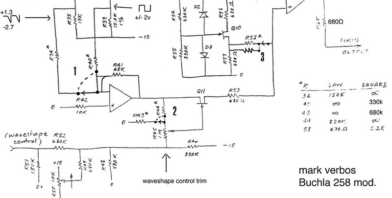
There are a few test points indicated on Mark Verbos' mutant build, in the waveshaping section, which is the same as the original. Signal levels may be different? You can slow down the oscillator with a positive voltage to the CV input and setting the attenuator in the "negative" counter-clockwise range, far enough down to be able to use a VOM (DC voltage setting) to see the wave cycle and its attendant peak-to-peak voltage readings.
http://www.simple-answer.com/258mod.jpg
FURTHER MODS
Verbos notes an inverted, negatively offset spike wave just off of two resistors in the waveshaping section (which is the same on the stock Buchla oscillators) :
http://www.simple-answer.com/258mod.jpg
This might be inverted, offset, and buffered to use as an audio signal (you would have to add an output buffer as was done for the triangle wave, or cut a trace and use the triangle buffer section for the spike).
The square wave can indeed be tapped per oscillator from one side of R39 prior to the sine/alt waveform mix circuitry, but would also require an opamp to buffer it for output.
EXTRA SPECIAL THANKS
goes to Dr. Tim Stinchcombe and Scott Stites and finally Don Buchla for the freaking great instruments! Regards!
RELATED PAGES
Info on parts and tolerances; the first link is highly recommended:
Buchla 258B Remake Project
Carbon Composition Resistors in Buchla Gear
Buchla 158A, 158B, 158 CBS versions
Cat